|
How about something like this[^]?
I'm not sure how many cookies it makes to be happy, but so far it's not 27.
JaxCoder.com
|
|
|
|
|
I wish it were that easy, but setting up the tiny computer as USB host is even more complicated.
I have lived with several Zen masters - all of them were cats.
His last invention was an evil Lasagna. It didn't kill anyone, and it actually tasted pretty good.
modified 1-Jul-20 10:16am.
|
|
|
|
|
I know it's complicated but this [^] might help.
I'm not sure how many cookies it makes to be happy, but so far it's not 27.
JaxCoder.com
|
|
|
|
|
Quote: it includes no PC host USB driver development facilities
Sounds like the microcontroller is set up as USB client with a PC as host. I would have to set up my coputer as the host, and that might be a little more complicated. Let me first build something that can load and boot an operating system before I write the OS itself.
I have lived with several Zen masters - all of them were cats.
His last invention was an evil Lasagna. It didn't kill anyone, and it actually tasted pretty good.
|
|
|
|
|
Never used LUFA and know little about it but I have seen a lot of people use it and thought it might help.
I'm not sure how many cookies it makes to be happy, but so far it's not 27.
JaxCoder.com
|
|
|
|
|
I doubt that any older 8 bit CPUs would make a good USB host. The old UARTs or USARTs don't even support the minimum bit rates and even with DMA you would struggle to get that stream of bytes through the bus in real time. Clients like a USB mouse or keyboard, which only snd a few bytes at a time, may be ok, but nothing that sends larger streams. As cool as USB might be, but I'm not sure if the effort to build it would be worth it, even if the lower bit rates are a lesser problem.
I have lived with several Zen masters - all of them were cats.
His last invention was an evil Lasagna. It didn't kill anyone, and it actually tasted pretty good.
|
|
|
|
|
CodeWraith wrote: And I would waste half of the drive's space.
With today's large drives, wasting half of the drive's space isn't a major issue today. The question is compatibility - (1) will any platform other than yours be able to read the disk, and (2) do you care?
I'm sure that circuit diagrams exist for the PC/XT's 8-bit disk controller and for other disk controllers of the same vintage. If that supported disks with a 16-bit bus, could you not cobble up something based on them to perform the 8-bit to 16-bit transfer?
Freedom is the freedom to say that two plus two make four. If that is granted, all else follows.
-- 6079 Smith W.
|
|
|
|
|
Quote: The question is compatibility
My 'drives' will probably be Compact Flash memory cards. It would be really nice to do all the software develpment on a PC, copy the results to the memory card and then plug it into the 8 bit computer.
Quote: I'm sure that circuit diagrams exist for the PC/XT's 8-bit disk controller and for other disk controllers of the same vintage. If that supported disks with a 16-bit bus, could you not cobble up something based on them to perform the 8-bit to 16-bit transfer?
It's absolutely simple. You just did not hook up the data lines you did not have. The upper half of a 16 bit word would simply not be used. The controller would not know about it and simply write or read these upper bits to the drive anyway. That's the point where you lose half of your disk's capacity.
I have lived with several Zen masters - all of them were cats.
His last invention was an evil Lasagna. It didn't kill anyone, and it actually tasted pretty good.
|
|
|
|
|
You may add two extra processors to read and store the upper and the lower bytes for you...
These two may work as a DMA toward the disk for your main processor...
"The only place where Success comes before Work is in the dictionary." Vidal Sassoon, 1928 - 2012
|
|
|
|
|
That's an idea. Holy overkill. Little 1802 says no to that. It never lets go of its bus for anything. Instead of simple 'shut up, processor' type DMA, it alwayskeeps running its program and throws in an extra DMA cycle with every instruction as long as DMA is requestet. It does all memory addressing itself and the requesting device just has to put its byte on the bus at the right moment. Two of them would start to scratch each other's eyes out.
Another thought: I can't really believe that they wastet half of a drive in the old days, just because you happened to have an 8088 processor. These drives where small and cost more than their weight in gold. Maybe there is something in the IDE drive's controller, perhaps in the control register, to tell it that we are running on only 8 cylinders.
I have lived with several Zen masters - all of them were cats.
His last invention was an evil Lasagna. It didn't kill anyone, and it actually tasted pretty good.
|
|
|
|
|
Talking of overkill... You mentioned the 1451... It had a 6502 inside just the same run the whole C64...
Maybe some shif-registers on the data lines can help you out?
"The only place where Success comes before Work is in the dictionary." Vidal Sassoon, 1928 - 2012
|
|
|
|
|
The processor board on the C64's floppy controller board had a little more to do, so it actually was not overkill.
For one thing, it controlled the stepper motors of the drive and the analog signal to the head directly. Look at other disk controller boards of that time (which could control several drives) and you can see that it was not a bad idea to put a separate processor on the controller board and let the computer's main processor do something else in that time. Each drive had its own controller, so multiple floppies could also work at the same time, unlike when you have only one processor and a central controller.
And then they did something really good: The processor on the controller also handled the file system. Indeed, the entire disk operating system of the C64 ran on the controllers, not the computer. The computer just sent DOS commands over a serial port and received the results the same way and otherwise needed no proccessor time or memory, both not overly abundant on a C64. And it could still have multiple drives working at the same time without additional cost.
Overall, it was very slow, but not because the concept was bad. The serial connection had a hardware bug, which was discovered when production had already started. The best thing they could do at that time was to do a quick software patch on the units that were already built, which was awfully slow. later they had to stay compatible to their older hardware and had to keep it that way, so it was officially never corrected. not even when the hardware bug had been fixed and newer drives could have been significantly faster.
I have lived with several Zen masters - all of them were cats.
His last invention was an evil Lasagna. It didn't kill anyone, and it actually tasted pretty good.
|
|
|
|
|
TurboDisk to the rescue!
Software bolt-on that increased floppy loads by a factor of 10.
The original version I had was a Basic program typed out of a magazine that would load some asm code to a fixed address. I disassembled it and figured out which op codes to tweak to load it wherever I wanted. C64 was a great learning machine.
|
|
|
|
|
Is there an SPI interface on your processor? might be easier to use SD cards...
|
|
|
|
|
No, the processor is from 1976. But a PIC microcontroller could actually help. Onw with a PSP, a USART for SPI and plenty of I/O pins. The old processor would talk to the PIC over the PSP, SD cards would be hooked up to the USART in SPI mode and the normal IO pins would be used for the IDE interface. There is even a library for the FAT32 file system, so that the PIC could also take care of all that.
I even have o suitable PIC here, but the IDE does not support it.
I have lived with several Zen masters - all of them were cats.
His last invention was an evil Lasagna. It didn't kill anyone, and it actually tasted pretty good.
|
|
|
|
|
|
Little CDP1802 never needed a DMA controller. Indeed, at no time it gives up control of the bus for any other devices, nor does it ever stop executing instructions. Instead, it throws in an extra bus cycle with every instruction when DMA is requested, does all the memory addressing itself and signals the device to put its byte onto the data bus or take it from the data bus. It is its own DMA controller and allows DMA for devices that normally would not be able to control the bus themselves.
On top of that, it also has another operating mode, the load mode. If you switch the processor into load mode after a reset, it will not execute any instructions, but serve DMA requests. This was used to read from the hex keyboard and at the same time to output the byte you had entered on the LED display. This way you could enter and run programs without any software and only simplest hardware involved.
I have lived with several Zen masters - all of them were cats.
His last invention was an evil Lasagna. It didn't kill anyone, and it actually tasted pretty good.
|
|
|
|
|
The only side I want to be on is the winning side.
|
|
|
|
|
Don't worry if you are on my side. I have found a schematic for an 8 bit IDE controller that actually is a good compromise. It does not waste half of your space, does not appear to be too slow and does not go overboard on the hardware side. Sadly, this also rules out DMA because DMA is still only works with the 8 bit data bus. That can't be changed.
I have lived with several Zen masters - all of them were cats.
His last invention was an evil Lasagna. It didn't kill anyone, and it actually tasted pretty good.
|
|
|
|
|
Quote: Ok, then it's good old parallel ATA/IDE. The problem here is that even the oldest specification requires a 16 bit data bus. You can use it with an 8 bit bus, but then the upper 8 bits of every 16 bit word would be wasted
Unless you have enough time to get the whole word with a mux.
|
|
|
|
|
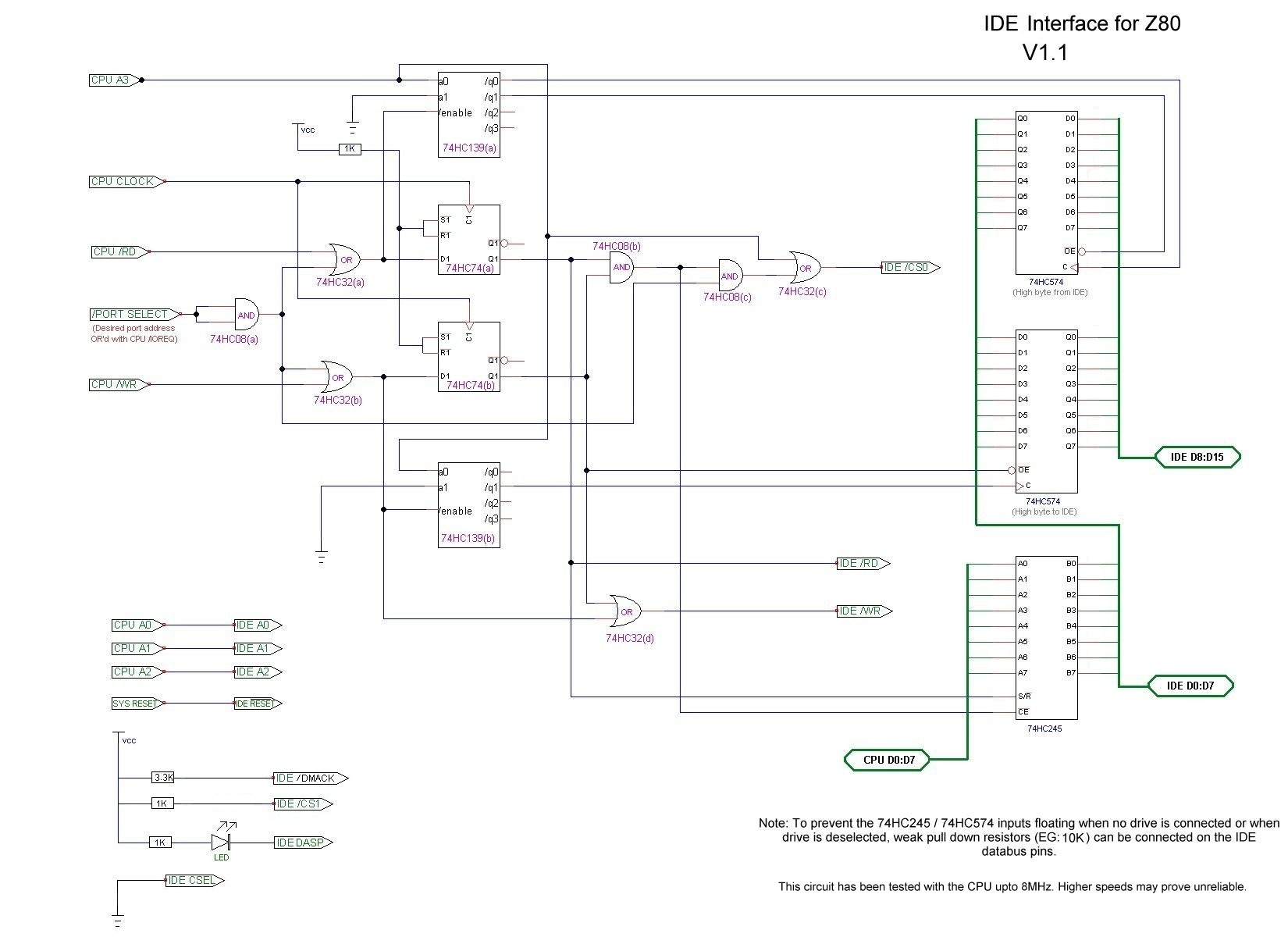
Or a 8 bit register/latch. The only complication is that both have to work bidirectionally and DMA on the 8 bit side is out of the question. I have found a schematic for a controller, designed for a Z80 system. It uses latches for the upper half of the data word and the direct approach (a bidirectional bus driver) for the lower half. A good compromise. Less sacrifice, still a victory.
Here is a link: http://blog.retroleum.co.uk/gfx/v4_ide_interface_schematic.jpg[^]
The schematic is kind of small, but you can enlarge it by clicking on it. Now I only have to adapt the logic that enables the out puts of the latches and bus drivers or when the latches have to store their data bits. The z80 does these things a little differently than my processor, but that should not be much of a problem.
I have lived with several Zen masters - all of them were cats.
His last invention was an evil Lasagna. It didn't kill anyone, and it actually tasted pretty good.
|
|
|
|
|
|
Hello. Sorry about the big block of text.
You mentioned the CDP1802 and, from what I read, it already has 16bit address but they are time multiplexed in 8bit. The best you can have is to insert an 8bit flip-flop to store the high 8bit of the address (or the low 8bit, whichever is sent first). There is probably some signal (pin or pins) that it uses to indicate when the first 8bit are sent and when the second 8bit are sent. You will need that to synchronize storing the address (allowing/disallowing writing to the flip-flops).
Keep in mind that, with 16bit, the most memory you can address is 65536 positions of 8bit, or 64kB.
Filesystem wise you have to go with something supporting at most 16 bit, like FAT16. Anything 32bit, like FAT32, is off the table since you would have to emulate the 32bit processing and that would most certainly kill performance. Even FAT16 might not run very fast or at all.
My recommendation would be for you to implement a raw flat filesystem. Think of the storage device as a fixed length file that has two lists, one starting at the lowest address and stores free positions of storage and positions of the start of the files (and maybe data like names, dates,etc), and another list starting at the highest address with the content of the files stored in reverse order (it is less problematic to expand files to free storage positions assuming you leave free space after each file). If you don't like the content in reverse order switch the positions of the two lists, in which case the first list will be in reverse order.
On a computer, you would have to either write a program that could handle this custom filesystem or write a FUSE layer to handle it seemingly. Writing a program that simply exports/imports all files from/to the filesystem to the filesystem of the computer is the easiest.
Advanced tip on expanding storage by using more flip-flops if both the CPU and storage device supports the timing: setup four flip-flops (remember these are 8bit wide) in the following manner: The first will store the high 8bit of the first address. The second will store the low 8bit of the first address. The third will store the data of the first address. The fourth will store the high 8bit of the second address. The low 8bit of the second address is pass-through.
Now you can use this trick to address up to 40bit worth of storage positions. Independently of you wanting to read or write to storage, first do a write with the high 16bit part of the address (bit 0 to 15) as the address and the 8bit data as the next 8bit of the address (bit 16 to 23). Next do the actual read/write from storage by passing the low 16bit of the address (bit 24 to 39) as the address.
If you need even more storage, you can add one more write using three extra flip-flops and use it as a block addresser. This would allow you to address 40bit storage positions of 24bit blocks or 48bit storage positions with 16bit blocks depending how you want to view it.
I have done something similar a long time ago with an 8051 and a 256MB disk.
Good luck 
|
|
|
|
|
Quote: You mentioned the CDP1802 and, from what I read, it already has 16bit address but they are time multiplexed in 8bit. The best you can have is to insert an 8bit flip-flop to store the high 8bit of the address (or the low 8bit, whichever is sent first). There is probably some signal (pin or pins) that it uses to indicate when the first 8bit are sent and when the second 8bit are sent. You will need that to synchronize storing the address (allowing/disallowing writing to the flip-flops).
You are right, latching the upper address bits is the first thing that's done in every bus cycle. Originally there were quite a few RAM and ROM chips that took only 8 address bits and the timing signal to latch the 16 address bits internally. These devices are now too small, too slow and almost impossible to get in any useful numbers, so an external latch has always been the standard. In the past this would have been a pair of 74C174s Or 40XX (CMOS!) or now (glimpsing at the breadboard) a single 74HC373.
Unfortunately we are talking about the data lines, not the address lines. The processor does not multiplex the data bus in any way. It's a strictly 8 bit CPU, quite unusual for a RISC processor.
Look at this IDE port for Z80 systems: An 8-bit IDE interface @ Retroleum[^]
That looks like a good compromise. Two reads or writes for every access to the disk controllers, once to the latches for the upper 8 data bits and a second one for the lower data bits to the bus 'HC245 bus driver. I need to adapt the decoding logic a little, because everything is done the Z80 way, but that's no real problem. Bit banging on a parallel port would be much slower and just ignoring the upper data bits would be extremely wasteful.
ElectronProgrammer wrote: Keep in mind that, with 16bit, the most memory you can address is 65536 positions of 8bit, or 64kB.
I expanded the address bus a little to 24 bit. So make that 16 Mb. 32 bit would also be no problem. Nothing special, just paged memory. A little detail of the processor's way to call subroutines allows me to hide the page switching, so that I can call code anywhere in that space without the processor noticing anything. Unfortunately that does not work for data, the stack, DMA or interrupts. For that, the page registers would have to be part of the processor.
ElectronProgrammer wrote: On a computer, you would have to either write a program that could handle this custom filesystem or write a FUSE layer to handle it seemingly. Writing a program that simply exports/imports all files from/to the filesystem to the filesystem of the computer is the easiest.
First things first. I will just get this working on the first prototype on the breadboard. Then I can build the second one with expanded memory (just 1 meg.  )and (hopefully) some mass storage device. Once that is built, I can still worry about the OS, the file system or comfort. )and (hopefully) some mass storage device. Once that is built, I can still worry about the OS, the file system or comfort.
I have lived with several Zen masters - all of them were cats.
His last invention was an evil Lasagna. It didn't kill anyone, and it actually tasted pretty good.
|
|
|
|
|
The 74HC373 are similar to the kind of chips I used in my 8051 school project but it was a couple octal D flip-flops instead of latches because we really don't need the two inputs, set and reset, and it took less board space (less pins). Maybe 74HC574 or similar but I don't really remember. Maybe there are chips for 16bit now.
The 8051 I used is similar to the CDP1802 you are using. It had 16bit addresses multiplexed in 8bit and 8bit data without multiplexing. It had no type of memory management. Only supported instructions to read/write registry or external address with the first block of external addresses taken by the internal memory.
I do remember that I expanded the address from 16bit to 32bit and the data I used both 8bit and 32bit. The drive I used had a 32bit block mode that read 8bit at a time in burst.
Expanding the data bus, from the hardware point of view, is identical to expanding the address bus with just one difference. The data bus is bidirectional so you need flip-flops (or latches) facing each direction of communication, they need to have an high impedance output when not enabled and care must be taken to select the correct facing flip-flops.
That is basically what is shown in the link you posted. However, the circuit I used was a little simpler but used more wires. The circuit in the link appears to "shift-register" the data from the two 74HC574 via the 74HC245 to the CPU.
In my circuit I just had all 74HC574 connected to the bus and just enabled the one I wanted to read/write. I had that "chip enabling" automated by using an extra shift-register that would shift a single one and was reset at the beginning of every read/write. And disabled the write chips by negating the read/write pin.
Like you said, is just more reads or writes from the CPU perspective. But still faster than parallel port and way faster than the serial port I had to use in the project that followed.
1MB? That's luxury 
It's almost as much RAM as my favourite laptop has (compaq contura aero 4/25 with 4MB) 
|
|
|
|
|


 General
  News
News  Suggestion
  Question
  Bug
Bug  Answer
  Joke
Joke  Praise
  Rant
Rant  Admin
Admin 


